Discover the path to ultra-cool, compact, and efficient fast charging with the world’s most efficient 65W USB-C reference design from Pulsiv

The demand for USB-C is forecast to surge over the next decade, fuelled by the migration from USB-A to USB-C and a growing market of portable devices that require fast charging. As power requirements increase, the need to deliver more power in a confined space adds challenges with thermal management and heat dissipation which impact safety and reliability. The PSV-RDAD-65USB reference design has been developed to demonstrate how Pulsiv OSMIUM technology reduces component temperatures, enabling products to consume less power and reduce overall size. It represents the first in a series of designs aimed at pushing the boundaries of power conversion to create a sustainable platform for the USB-C standard.
In this design, the Pulsiv OSMIUM microcontroller PSV-AD-65EG-Q24IV has been combined with OnSemi’s NCP1342 Flyback controller and GaN devices from Innoscience to deliver a world leading specification:
Input Voltage Range: 90 – 265VAC
(no input voltage derating)
Output Voltage: 5 – 20VDC supporting PD3.0, QC4.0, BC1.2, & PPS (Fast Charging)
Output Power: 65W max
Transformer Temperature: 30.3°C above ambient
Operating Frequency: 125kHz
Peak Efficiency: 96%
Average Efficiency: 95%
Half-Active Bridge: Included
Line Currents: 0.5A max
Inrush Current: Eliminated
GaN Optimised: Yes
DC-DC Converter: Quasi-Resonant (QR) Flyback
Taking ultra-cool operation & fast charging to a whole new level
Critical components in conventional designs will often reach temperatures of over 100°C, so measures must naturally be taken to dissipate heat or limit output power. This means compromising cost, performance, or physical size to mitigate safety and reliability issues.

Competitor data demonstrates a highest component temperature of 93.6°C
A 65W USB-C reference design from a leading manufacturer of power supply solutions.
NOTE: The thermal data shown has been taken from their datasheet in the public domain
The Pulsiv OSMIUM reference design demonstrates a significant improvement in thermal performance and reduces critical component temperatures by more than 30% compared to other designs. At full load, the Flyback transformer reaches an impressive 33.9°C at 230VAC and 30.3°C at 265V above an ambient temperature of 26.1°C. This incredible achievement is likely to set a new benchmark and enables 65W fast charging in space constrained environments and/or heat sensitive applications such as in-wall plug sockets that incorporate USB-C connectivity.

Thermal measurement of the Pulsiv PSV-EBAD-65USB evaluation board demonstrates the hottest component temperature of 62.7°C
Pulsiv PSV-EBAD-65USB Evaluation board:
Vin = 230VAC, Vout = 20V, Iout = 3.25A, 26.1°C ambient
Setting a new benchmark in power conversion
Pulsiv OSMIUM technology is a patented AC to DC front-end conversion method that applies intelligence to an active valley fill approach and delivers a combination of game changing benefits in power electronics designs. It significantly improves performance at low loads to increase overall average efficiency, reduce energy consumption, and deliver a totally flat efficiency profile across all load conditions.
The Pulsiv AC to DC conversion method intelligently regulates the charging current and voltage on the storage capacitor using a high-side architecture to switch Qch. This allows the use of 200V or 160V capacitors (selectable) to support a universal mains input. The valley-fill period is broadly similar to a 2C3D architecture; but the charging period of the capacitor is significantly longer and more variable.

Pulsiv OSMIUM high side architecture
Reducing system losses
Figure 1 shows a simplified circuit implementation to illustrate the basic operation of Pulsiv OSMIUM technology in this design. A MOSFET, Qch, is used to control the charging of Cch to generate a configurable high-voltage DC output (HVDC) and a blocking diode Db ensures that Cch does not discharge through the body diode of Qch while avoiding stray conduction through the inductor. This approach allows the use of smaller and lower cost 200V or 160V capacitors to support a universal mains input.
Losses during the charging phase are typically between 0.5% and 2%, resulting in a peak efficiency of up to 99.5%. The circuit converts just enough energy to maintain capacitor voltage and delivers consistent efficiency over the full power range.
In a traditional valley-fill design, AC to DC conversion involves a full-wave diode bridge. Diode losses are mainly determined by the average current, RMS current, the forward voltage drop, and the resistance during conduction. Conventional systems without power factor correction exhibit large peak currents, resulting in higher RMS currents and greater diode bridge losses. Power factor correction improves RMS current and results in a current waveform with a crest factor of √2. Pulsiv OSMIUM designs typically have a crest factor of 1.3, which is lower than that of a sinusoid, leading to lower RMS values and reduced losses. Peak line currents are reduced by up to 90% as a direct result of the way Pulsiv OSMIUM controls capacitor charging, and inrush current is also eliminated.

Typical Line Currents
Optimize efficiency and space with a half-active bridge
Pulsiv OSMIUM technology senses AC line voltage and frequency to adjust capacitor charging time, therefore the circuit draws no line current at the AC zero voltage crossing. This enables a simple half-active bridge implementation to increase efficiency, especially at low line conditions. MOSFETs in the lower half of the AC to DC bridge are carefully controlled, in combination with high-side diodes. The half-active bridge in this design strikes the delicate balance between efficiency, cost, and complexity and supports universal input with efficiency gains of 0.7% at full load from a 115V AC supply.

Pulsiv unique Half-Active Bridge Control
Innovation in magnetics design reduces transformer size by 20%
Pulsiv OSMIUM technology generates a HVDC output that varies between the peak AC input and 150V (with a 230V input) to drive the QR Flyback at maximum efficiency. The wide voltage range it generates requires a significantly reduced primary side inductance which enables the use of an EQ20 transformer. This was developed in partnership with magnetics experts Frenetic where a 20% size reduction was achieved compared to the typical RM8 used in other designs.


Minimizing losses with GaN optimization
GaN transistors from Innoscience were used to lower the RDSon which reduced conduction losses, but this naturally increased parasitic capacitance. The INN700DA240B was the optimum device which provided the necessary balance between the two losses. An additional Innoscience GaN transistor INN150FQ032A was also selected to provide the most suitable match for operating with the synchronous rectifier controller and output current from the transformer.
In this design, GaN lowered the overall energy consumption, reduced component size, and improved cost compared to conventional MOSFET’s. Innoscience also provided outstanding support, delivering samples within 48hrs, and demonstrating the most competitive pricing.
Design package & evaluation boards
The PSV-RDAD-65USB document package is available to download free from the Pulsiv website and includes a Datasheet, Schematics, Bill of Materials, & Altium files. The PSV-EBAD-65USB evaluation board enables rapid lab testing and can be pre-ordered now for delivery in the 2nd half of August through a network of franchised distribution partners including global stockist Digikey.
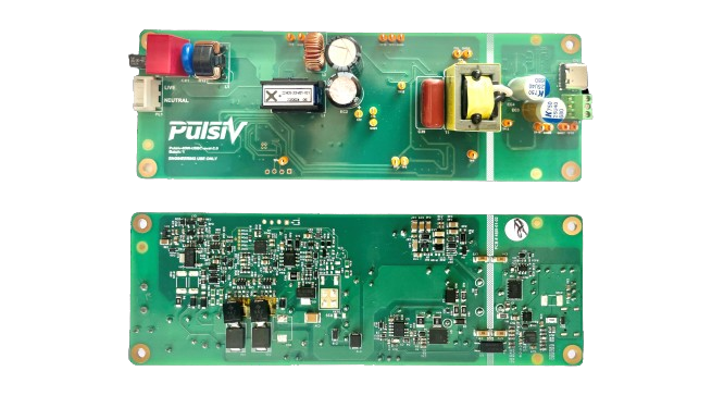
PSV-EBAD-65USB Evaluation Board
Summary
The PSV-RDAD-65USB reference design showcases a truly sustainable approach to efficient power conversion, ultra-cool thermal performance, and reduced energy consumption in USB-C applications. It demonstrates how the unique Pulsiv OSMIUM technology can influence magnetics design while supporting GaN to minimize overall losses. Its game-changing thermal performance enables USB-C to be adopted quickly and safely while paving the way for fast charging within virtually any application.
Fully assembled, size optimized, and EMC compliant “Plug & Play” modules of this reference design are currently under development which aim to accelerate adoption and simplify the design process. They will offer configurations of 1C, 1C1A, and 2C1A with other variants possible and can be pre-ordered through any of the franchised distribution partners for expected delivery in Q4 2024.